Glitching: Difference between revisions
No edit summary |
No edit summary |
||
| (13 intermediate revisions by the same user not shown) | |||
| Line 7: | Line 7: | ||
[[File:vita_nand_testpoint_1.jpg|thumb|eMMC pinout]] | [[File:vita_nand_testpoint_1.jpg|thumb|eMMC pinout]] | ||
Use 28AWG wire to solder directly to the termination resistor. There are no testpoints. For the clock signal, | Use 28AWG wire to solder directly to the termination resistor. There are no testpoints. For the clock signal, you should solder to the yellow point if you are using the latest psvemmc. Older versions have a bug that prevent the clock from being driven correctly. In that case, you have to use the orange point if you wish to probe the signal. If you solder to the yellow point, you can flash but not boot up the Vita. This has been fixed in psvemmc v3.1 and you no longer need to use the orange point at all. | ||
You need the Vita to power the eMMC so it has to be turned on before you can attach an external adapter. However, the Vita will not stop trying to drive the eMMC clock until after boot is done. This means you should not try to connect an external adapter until after the Vita is idling in shell or safe mode. If you are not able to boot into either modes, an alternative is to hold Kermit in reset. The pulldown resistor for RESET_N is boxed in yellow. | You need the Vita to power the eMMC so it has to be turned on before you can attach an external adapter. However, the Vita will not stop trying to drive the eMMC clock until after boot is done. This means you should not try to connect an external adapter until after the Vita is idling in shell or safe mode. If you are not able to boot into either modes, an alternative is to hold Kermit in reset. The pulldown resistor for RESET_N is boxed in yellow. | ||
[[File:reset_pinout.png|thumb|RESET_N]] | [[File:reset_pinout.png|thumb|RESET_N]] | ||
== Clocks == | |||
If you only remove the crystal, you can control the [http://www.onsemi.com/PowerSolutions/product.do?id=P1P40167 P1P40167] clock synthesizer from it. From experiments, it seems like each clock output has a linear relationship with the crystal input frequency down to about 4MHz. You can get better results by removing the clock synthesizer and feeding your external clock directly to pin 3 (48M clock for eMMC) and pin 11 (37M clock for Kermit). By synchronizing these two clocks together, you can also get more consistent results with eMMC trigger for glitching. The other two clock outputs can be left floating and the Vita will still boot. | |||
== ChipWhisperer == | == ChipWhisperer == | ||
=== psvemmc Target === | === psvemmc Target === | ||
[https://github.com/yifanlu/psvsd/tree/master/psvemmc psvemmc v2.0+] has an interface for connecting the chipwhisperer lite through a 20-pin connector. | [https://github.com/yifanlu/psvsd/tree/master/psvemmc psvemmc v2.0+] has an interface for connecting the chipwhisperer lite through a 20-pin connector. There is a jumper JP1 that places the SD to USB IC in reset. JP1 must be selected and a USB cable must be connected (for the 1.8V VTarget) to interface with chipwhisperer. Remove the jumper to drive the eMMC from the adapter and enable USB data (see notes above for when you can do this). | ||
{| class="wikitable" | {| class="wikitable" | ||
| Line 42: | Line 46: | ||
| CLK_IN | | CLK_IN | ||
| I/O | | I/O | ||
| EXT_CLK input to CW | | EXT_CLK input to CW (can be left unconnected) | ||
|- | |- | ||
| 5 | | 5 | ||
| Line 72: | Line 76: | ||
| UART_TX | | UART_TX | ||
| I/O | | I/O | ||
| TargetIO Pin 1 - UART TX | | TargetIO Pin 1 - UART TX (=> RX on Vita) | ||
|- | |- | ||
| 11 | | 11 | ||
| Line 82: | Line 86: | ||
| UART_RX | | UART_RX | ||
| I/O | | I/O | ||
| TargetIO Pin 2 - UART RX | | TargetIO Pin 2 - UART RX (=> TX on Vita) | ||
|- | |- | ||
| 13 | | 13 | ||
| Line 128: | Line 132: | ||
|} | |} | ||
The eMMC and RESET_N pins are diagramed above. | The eMMC and RESET_N pins are diagramed above. You should solder GND from the Vita to the molecule logo (which is actually a pad). For best performance (from experimentation), solder a short wire from the shield frame near the eMMC clock resistor and a short wire from any GND pad near the Kermit 37M clock to the molecule logo. Other pinouts are listed below. | ||
[[File:power_pinout.png|thumb|PWR_SW]] | [[File:power_pinout.png|thumb|PWR_SW]] | ||
| Line 136: | Line 140: | ||
[[File:Vita-syscon-spi.png|thumb|Kermit <-> Ernie SPI]] | [[File:Vita-syscon-spi.png|thumb|Kermit <-> Ernie SPI]] | ||
[[File:Vita-vdd12-cap. | [[File:Vita-vdd12-cap.jpg|thumb|Glitch VDD12 (left: VDD12, right: GND)]] | ||
[[File:Vita-37M-clk.png|thumb|37M CLK_OUT (remove the IC)]] | |||
==== Soldering Tips ==== | |||
The recommended way is to use a stencil, but if you don't have that, here's some advice from hours of painstaking experiences. First, apply some solder to all the passive component pads. Either use a tip-pointed solder iron and melt a small blob on each pad or spread some blobs of solder paste liberally in a couple areas of a board and use a blade tipped solder iron to spread the melted solder across all the pads. Then place the passives down and use a hot air gun to melt them in place. | |||
Next are the ICs. First, get rid of any excess solder on the center pads with an air pump. If you don't, then after putting the ICs on, they might overflow onto the legs and cause shorts. The easiest way I've found to make sure the ICs are soldered correctly is to put a line of paste on each row of legs and then use a blade tipped iron to melt the solder in place by pressing the tip on the entire row at once. Any excess solder will stick to the tip automatically. If there are shorts, clean the blade tip and press against the row again. This should ensure an even distribution of solder on all the legs. Then put the IC in place and use a hot air gun to melt the solder. After it is melted, you may want to use a tweezer to apply pressure evenly on the chip (for example press against two opposite corners of the IC at once with your tweezer) and hold it there after moving the hot air gun away for a couple of seconds to ensure connectivity. Note that if you have excess solder on the center pads, they will now overflow to the legs and you may see shorts. If this happens, remove the IC, and start over. | |||
After you are done, check that there's not any shorts with a multi meter. The most important points to check are the pads on the LDO. If pins 4 or 5 gets shorted, you WILL kill the LDO. Many LDOs died because of this. Make sure pins 4 and 5 are not shorted to each other or any other pins. The easy way to check is to look at C4 and C5 and make sure the non-ground side is not shorted to +5V, +3.3V, +1.8V, or GND. Then check that none of the voltage input/output pins are shorted to GND or each other. | |||
==== Troubleshooting Tips ==== | |||
# Make sure the USB port is soldered properly. Check +5V to C16, GND, and D+/D- to USB2244 pins 2-3. | |||
# Make sure +5V from USB protection IC goes to LDO. Check L1 for +5V. | |||
# Make sure LDO is outputting both +1.8V and +3.3V correctly. | |||
# Make sure !USB_EN is high (3.3V) | |||
# Using a scope, make sure the crystal is powered on (look for 24MHz on either side of R1). If not, there might be a problem with pin 35 (RBIAS), pin 32/33 (crystal), pin 18 (reset), or any of the power pins. Check that all the solder joints are correct. | |||
# Once all of the above is correct, you should see the USB device on your computer. Now reset the USB and immediately probe pin 9 of USB2244 and you should see an SD clock. Then probe pin 11 and you should see SD cmd traffic (after a second, the USB2244 will stop retrying so you may need to reset the USB multiple times while testing). If you don't see anything, check that pin 30 (SD_WP) is soldered correctly. Check that pin 5 (SD_D0) is high. | |||
# If all that is correct, then the USB2244 is working properly. Check soldering of the U3 next to make sure the level translator is correct. Check U5 to make sure the level translator enable logic is correct. Check U6 to make sure the clock level translator is correct. | |||
=== Hardware === | === Hardware === | ||
| Line 144: | Line 168: | ||
=== Software === | === Software === | ||
You must use the custom build of [https://github.com/ | You must use the custom build of [https://github.com/TeamMolecule/chipwhisperer chipwhisperer]. This build has the target IO restraints set to 1.8V as well as support for the MMC logger/trigger and UART trigger. Follow the installation instructions from [https://wiki.newae.com/Installing_ChipWhisperer newae] and you can execute the glitch scripts by copying them to "software/vita-glitching". | ||
Latest revision as of 22:14, 6 January 2019
eMMC
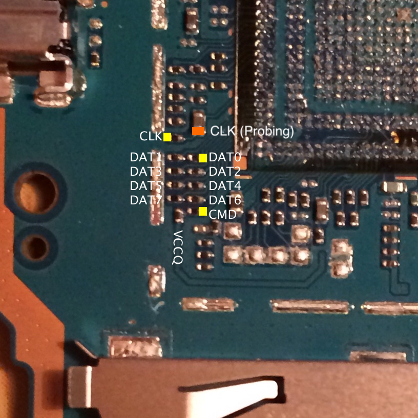
CMD, CLK, and DAT0 are needed to flash the eMMC. Note that the Vita uses 1.8V logic and most if not all SD card adapters use 3.3V logic so unlike other devices you cannot just solder to a standard SD card adapter! psvemmc v1.2+ contain level translation that allow you to safely interface with the Vita eMMC.
Connection
Use 28AWG wire to solder directly to the termination resistor. There are no testpoints. For the clock signal, you should solder to the yellow point if you are using the latest psvemmc. Older versions have a bug that prevent the clock from being driven correctly. In that case, you have to use the orange point if you wish to probe the signal. If you solder to the yellow point, you can flash but not boot up the Vita. This has been fixed in psvemmc v3.1 and you no longer need to use the orange point at all.
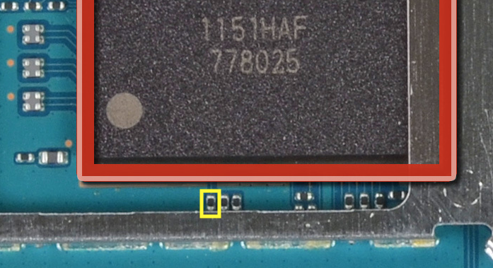
You need the Vita to power the eMMC so it has to be turned on before you can attach an external adapter. However, the Vita will not stop trying to drive the eMMC clock until after boot is done. This means you should not try to connect an external adapter until after the Vita is idling in shell or safe mode. If you are not able to boot into either modes, an alternative is to hold Kermit in reset. The pulldown resistor for RESET_N is boxed in yellow.
Clocks
If you only remove the crystal, you can control the P1P40167 clock synthesizer from it. From experiments, it seems like each clock output has a linear relationship with the crystal input frequency down to about 4MHz. You can get better results by removing the clock synthesizer and feeding your external clock directly to pin 3 (48M clock for eMMC) and pin 11 (37M clock for Kermit). By synchronizing these two clocks together, you can also get more consistent results with eMMC trigger for glitching. The other two clock outputs can be left floating and the Vita will still boot.
ChipWhisperer
psvemmc Target
psvemmc v2.0+ has an interface for connecting the chipwhisperer lite through a 20-pin connector. There is a jumper JP1 that places the SD to USB IC in reset. JP1 must be selected and a USB cable must be connected (for the 1.8V VTarget) to interface with chipwhisperer. Remove the jumper to drive the eMMC from the adapter and enable USB data (see notes above for when you can do this).
| Number | Name | Dir | Description |
|---|---|---|---|
| 1 | N/C | O | Not Connected |
| 2 | GND | O | System GND. |
| 3 | N/C | O | Not Connected |
| 4 | CLK_IN | I/O | EXT_CLK input to CW (can be left unconnected) |
| 5 | RESET_N | I/O | Kermit RESET |
| 6 | CLK_OUT | I/O | Clock from CW to Vita |
| 7 | SPI_MISO | I/O | SPI input: MISO |
| 8 | VTarget | I | Driven to +1.8V. |
| 9 | SPI_MOSI | I/O | SPI output: MOSI |
| 10 | UART_TX | I/O | TargetIO Pin 1 - UART TX (=> RX on Vita) |
| 11 | SPI_SCK | I/O | SPI output: SCK |
| 12 | UART_RX | I/O | TargetIO Pin 2 - UART RX (=> TX on Vita) |
| 13 | SPI_CS | I/O | SPI input: CS |
| 14 | MMC_CLK | I/O | TargetIO Pin 3 - eMMC CLK (probing) |
| 15 | PWR_SW | I/O | Vita power switch |
| 16 | MMC_CMD | I/O | TargetIO Pin 4 - eMMC CMD (probing) |
| 17 | GND | O | |
| 18 | N/C | O | Not Connected |
| 19 | GND | O | |
| 20 | N/C | O | Not Connected |
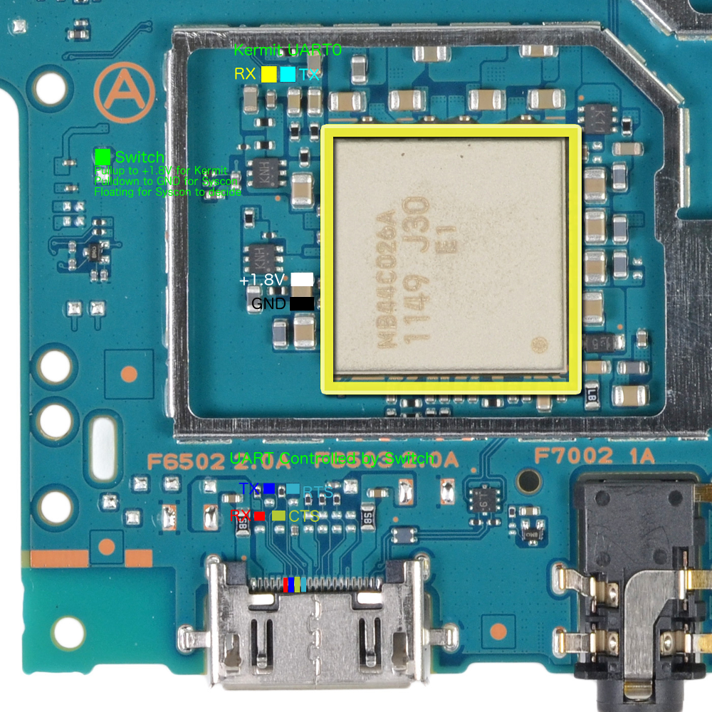
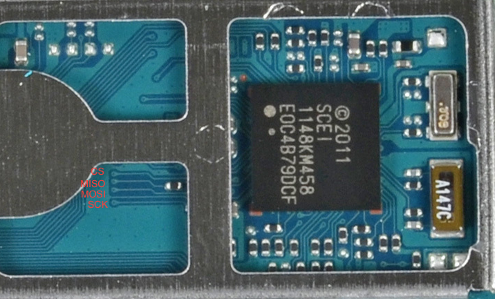
The eMMC and RESET_N pins are diagramed above. You should solder GND from the Vita to the molecule logo (which is actually a pad). For best performance (from experimentation), solder a short wire from the shield frame near the eMMC clock resistor and a short wire from any GND pad near the Kermit 37M clock to the molecule logo. Other pinouts are listed below.
Soldering Tips
The recommended way is to use a stencil, but if you don't have that, here's some advice from hours of painstaking experiences. First, apply some solder to all the passive component pads. Either use a tip-pointed solder iron and melt a small blob on each pad or spread some blobs of solder paste liberally in a couple areas of a board and use a blade tipped solder iron to spread the melted solder across all the pads. Then place the passives down and use a hot air gun to melt them in place.
Next are the ICs. First, get rid of any excess solder on the center pads with an air pump. If you don't, then after putting the ICs on, they might overflow onto the legs and cause shorts. The easiest way I've found to make sure the ICs are soldered correctly is to put a line of paste on each row of legs and then use a blade tipped iron to melt the solder in place by pressing the tip on the entire row at once. Any excess solder will stick to the tip automatically. If there are shorts, clean the blade tip and press against the row again. This should ensure an even distribution of solder on all the legs. Then put the IC in place and use a hot air gun to melt the solder. After it is melted, you may want to use a tweezer to apply pressure evenly on the chip (for example press against two opposite corners of the IC at once with your tweezer) and hold it there after moving the hot air gun away for a couple of seconds to ensure connectivity. Note that if you have excess solder on the center pads, they will now overflow to the legs and you may see shorts. If this happens, remove the IC, and start over.
After you are done, check that there's not any shorts with a multi meter. The most important points to check are the pads on the LDO. If pins 4 or 5 gets shorted, you WILL kill the LDO. Many LDOs died because of this. Make sure pins 4 and 5 are not shorted to each other or any other pins. The easy way to check is to look at C4 and C5 and make sure the non-ground side is not shorted to +5V, +3.3V, +1.8V, or GND. Then check that none of the voltage input/output pins are shorted to GND or each other.
Troubleshooting Tips
- Make sure the USB port is soldered properly. Check +5V to C16, GND, and D+/D- to USB2244 pins 2-3.
- Make sure +5V from USB protection IC goes to LDO. Check L1 for +5V.
- Make sure LDO is outputting both +1.8V and +3.3V correctly.
- Make sure !USB_EN is high (3.3V)
- Using a scope, make sure the crystal is powered on (look for 24MHz on either side of R1). If not, there might be a problem with pin 35 (RBIAS), pin 32/33 (crystal), pin 18 (reset), or any of the power pins. Check that all the solder joints are correct.
- Once all of the above is correct, you should see the USB device on your computer. Now reset the USB and immediately probe pin 9 of USB2244 and you should see an SD clock. Then probe pin 11 and you should see SD cmd traffic (after a second, the USB2244 will stop retrying so you may need to reset the USB multiple times while testing). If you don't see anything, check that pin 30 (SD_WP) is soldered correctly. Check that pin 5 (SD_D0) is high.
- If all that is correct, then the USB2244 is working properly. Check soldering of the U3 next to make sure the level translator is correct. Check U5 to make sure the level translator enable logic is correct. Check U6 to make sure the clock level translator is correct.
Hardware
The cwlite must be modified to support the +1.8V level required by the Vita target. First remove the solder bridge on SJ6, which forces the FPGA logic to 3.3V. Next solder some pin header to JP5 and place a jumper between pin 2 and 3 (the two pins farthest from the FPGA). This will allow the psvemmc target's 1.8V VTarget pin to be used.
Software
You must use the custom build of chipwhisperer. This build has the target IO restraints set to 1.8V as well as support for the MMC logger/trigger and UART trigger. Follow the installation instructions from newae and you can execute the glitch scripts by copying them to "software/vita-glitching".


