|
|
| Line 8: |
Line 8: |
| == Variants == | | == Variants == |
|
| |
|
| There are multiple known variants of Kermit. SoC revision is readable from [[Pervasive#.22SoC_revision.22|a ScePervasiveMisc register]]. | | There are multiple known variants of Kermit. SoC revision is readable from [[Pervasive#revision0|a ScePervasiveMisc register]]. |
|
| |
|
| The following table is split in two depending on the Kermit version (1.0 or 1.5). <code>X</code> and <code>Y</code> from the <code>ESXrY</code> column corresponds to the values in the SoC info register (<code>0x000000XY</code>). | | The following table is split in two depending on the Kermit version (1.0 or 1.5). <code>X</code> and <code>Y</code> from the <code>ESX.Y</code> column corresponds to the values in the </code>revision0</code> register (<code>0x000000XY</code>). |
|
| |
|
| {| class="wikitable" | | {| class="wikitable" |
| Line 19: |
Line 19: |
| ! colspan="4" | Kermit 1.0 | | ! colspan="4" | Kermit 1.0 |
| |- | | |- |
| | ES4r2 || CXD5315GG || PCH-1xxx, VTE-10xx || Retail unit, ?512MiB LPDDR2? | | | ES1 || ??? || DEM revision before DEM-3000G || CPU is Cortex-A8, GPU is SGX541MP, ?no CDRAM?. Has two minor revisions: ES1.0 and ES1.1 |
| |- | | |- |
| | ES4r2 || CXD5315GG-1 || PDEL-10xx || TOOL, ?1.5GiB LPDDR2? | | | ES2 || ??? || DEM-3000G? to DEM-3000H? || CPU is Cortex-A9, GPU is SGX543MP4+. Has only one minor revision: ES2.0. |
| |- | | |- |
| | ES1 || ??? || DEM revision before DEM-3000G || CPU is Cortex-A8, GPU is SGX541MP, ?no CDRAM? - only ES1r0 and ES1r1 should exist | | | ES3 || ??? || ?DEM-3000JEC, some DEM-3000K/J? || Has three minor revisions: ES3.0, ES3.1 and ES3.2 |
| |- | | |- |
| | ES2 || ??? || DEM-3000G ?to DEM-3000H? || CPU is Cortex-A9, GPU is SGX543MP4+ | | | ? || T9ML7MBG-S || CEM-3000VD1 || Units used for [https://fccid.io/AK8PCH1001A PCH-1001 FCC certification] and [https://fccid.io/AK8PCH1101A PCH-1101 FCC certification] uses this chip. Most likely ES4, probably ES4.2. |
| |- | | |- |
| | ES3 || ??? || ?DEM-3000JEC, some DEM-3000K/J? || Only ES3r0, ES3r1 and ES3r2 should exist | | | ES4.0 || ??? || ? || Known to exist from strings in a debugging <code>second_loader.bin</code> dated 2011/05/24, which implies that ES4.1 didn't exist at that point in time. |
| |- | | |- |
| | ? || T9ML7MBG-S || CEM-3000VD1 || Units used for [https://fccid.io/AK8PCH1001A PCH-1001 FCC certification] and [https://fccid.io/AK8PCH1101A PCH-1101 FCC certification] uses this chip. Most likely ES4, probably ES4r2. | | | ES4.2 || CXD5315GG || PCH-1xxx, VTE-10xx || Retail unit, ?512MiB LPDDR2? |
| | |- |
| | | ES4.2 || CXD5315GG-1 || PDEL-10xx || TOOL, ?1.5GiB LPDDR2? |
| |- | | |- |
| ! colspan="4" | Kermit 1.5 | | ! colspan="4" | Kermit 1.5 |
| |- | | |- |
| | ES1r5 || CXD5316GG || PCH-20xx || Unit used for [https://fccid.io/AK8PCH2001 PCH-2001 FCC certification] uses this chip. Some motherboards with this Kermit (<code>AU_CODEC_IC_CONEXANT</code> is true) use an IC from Conexant instead of Wolfson Microelectronics for audio codec. | | | ES1.5 || CXD5316GG || PCH-20xx || Unit used for [https://fccid.io/AK8PCH2001 PCH-2001 FCC certification] uses this chip. Some motherboards with this Kermit (<code>AU_CODEC_IC_CONEXANT</code> is true) use an IC from Conexant instead of Wolfson Microelectronics for audio codec. |
| |} | | |} |
|
| |
|
| Line 42: |
Line 44: |
| ! Erratum # !! Present on !! Fixed on !! Description | | ! Erratum # !! Present on !! Fixed on !! Description |
| |- | | |- |
| | 93 || Kermit ES1 || Kermit ES2 || The SDIO bus must not be set to High Speed due to a silicon bug. | | | 93 || Kermit ES1 || Kermit ES2 || The SDIO bus must not be set to High Speed due to a silicon bug.|} |
| |} | |
|
| |
|
| == Schema == | | == Schema == |
Revision as of 21:49, 19 April 2023
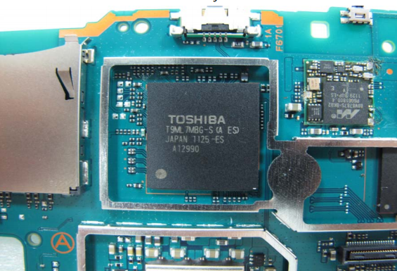
The PS Vita main SoC, nicknamed Kermit, is manufactured by Toshiba. The design is a stacked SoC with the SDRAM found in the same chip as the processor cores. Toshiba details their "Stacked Chip SOC" on their site.
More information can be found at Chipworks.

From FCC application 712137
According to the internal photos found in the FCC filings, it appears that an earlier version of the chip is labeled T9ML7MBG-S. This does not appear to be a standard model and is likely custom designed in partnership with Sony Computer Entertainment Japan. It is possible that Sony used this service from Toshiba in their design process which is why the prototype demonstrated in the FCC filing shows a Toshiba chip..
Variants
There are multiple known variants of Kermit. SoC revision is readable from a ScePervasiveMisc register.
The following table is split in two depending on the Kermit version (1.0 or 1.5). X and Y from the ESX.Y column corresponds to the values in the revision0 register (0x000000XY).
Known Kermit revisions
| Kermit revision |
SoC model number |
Unit model number |
Notes
|
| Kermit 1.0
|
| ES1 |
??? |
DEM revision before DEM-3000G |
CPU is Cortex-A8, GPU is SGX541MP, ?no CDRAM?. Has two minor revisions: ES1.0 and ES1.1
|
| ES2 |
??? |
DEM-3000G? to DEM-3000H? |
CPU is Cortex-A9, GPU is SGX543MP4+. Has only one minor revision: ES2.0.
|
| ES3 |
??? |
?DEM-3000JEC, some DEM-3000K/J? |
Has three minor revisions: ES3.0, ES3.1 and ES3.2
|
| ? |
T9ML7MBG-S |
CEM-3000VD1 |
Units used for PCH-1001 FCC certification and PCH-1101 FCC certification uses this chip. Most likely ES4, probably ES4.2.
|
| ES4.0 |
??? |
? |
Known to exist from strings in a debugging second_loader.bin dated 2011/05/24, which implies that ES4.1 didn't exist at that point in time.
|
| ES4.2 |
CXD5315GG |
PCH-1xxx, VTE-10xx |
Retail unit, ?512MiB LPDDR2?
|
| ES4.2 |
CXD5315GG-1 |
PDEL-10xx |
TOOL, ?1.5GiB LPDDR2?
|
| Kermit 1.5
|
| ES1.5 |
CXD5316GG |
PCH-20xx |
Unit used for PCH-2001 FCC certification uses this chip. Some motherboards with this Kermit (AU_CODEC_IC_CONEXANT is true) use an IC from Conexant instead of Wolfson Microelectronics for audio codec.
|
Errata
| Erratum # |
Present on |
Fixed on |
Description
|
| 93 |
Kermit ES1 |
Kermit ES2 |
}
Schema
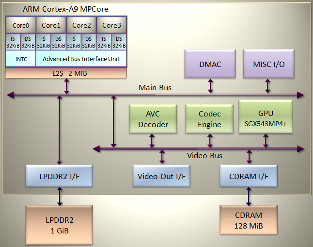
This is for DevKit. Retail and TestKit are different:
- The DevKit carries 1 GiB of LPDDR2 DRAM (usually referred to as the "main memory"). The retail unit and TestKit carry 512 MiB of LPDDR2 DRAM.

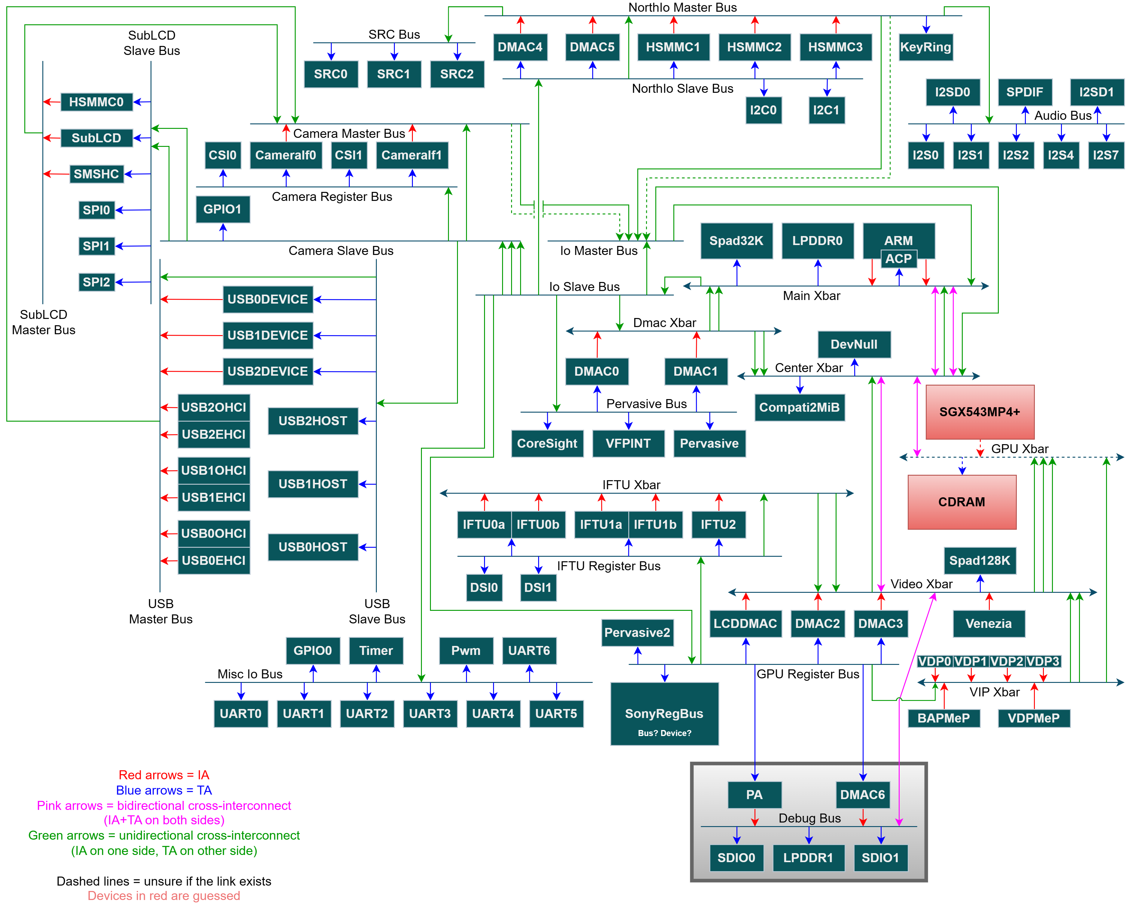
Thanks to information in a debug version of SceKernelBusError, the following bus diagram has been reconstructed:

CPU
See Main_Processor.
GPU
See SGX543.
LPDDR2 DRAM (main memory)
- The retail unit and TestKit carry 512 MiB of LPDDR2 DRAM.
- The DevKit carries 1 GiB of LPDDR2 DRAM (usually referred to as the "main memory").
Trace Memory
The DevKit mounts 512 MiB of LPDDR2 DRAM for performance analysis.
This memory is for storing performance measurement data referred by a performance analyzer (Razor for PlayStation®Vita) or runtime libraries.
Custom DRAM
The DevKit carries 128 MiB of custom DRAM (usually referred to as the "video memory"). ?Retail/TesKit too?
Codec Engine
Codec Engine is a media processor configured with multiple cores. Only the specific processing of the specific libraries is processed through Codec Engine instead of CPU.
Other Key Units and Bus Configuration
As other key units, the custom SoC includes the features below:
- Direct Memory Access Controllers (DMAC)
- AVC Decoder
- A video out interface
- Misc input/outputs interface etc.
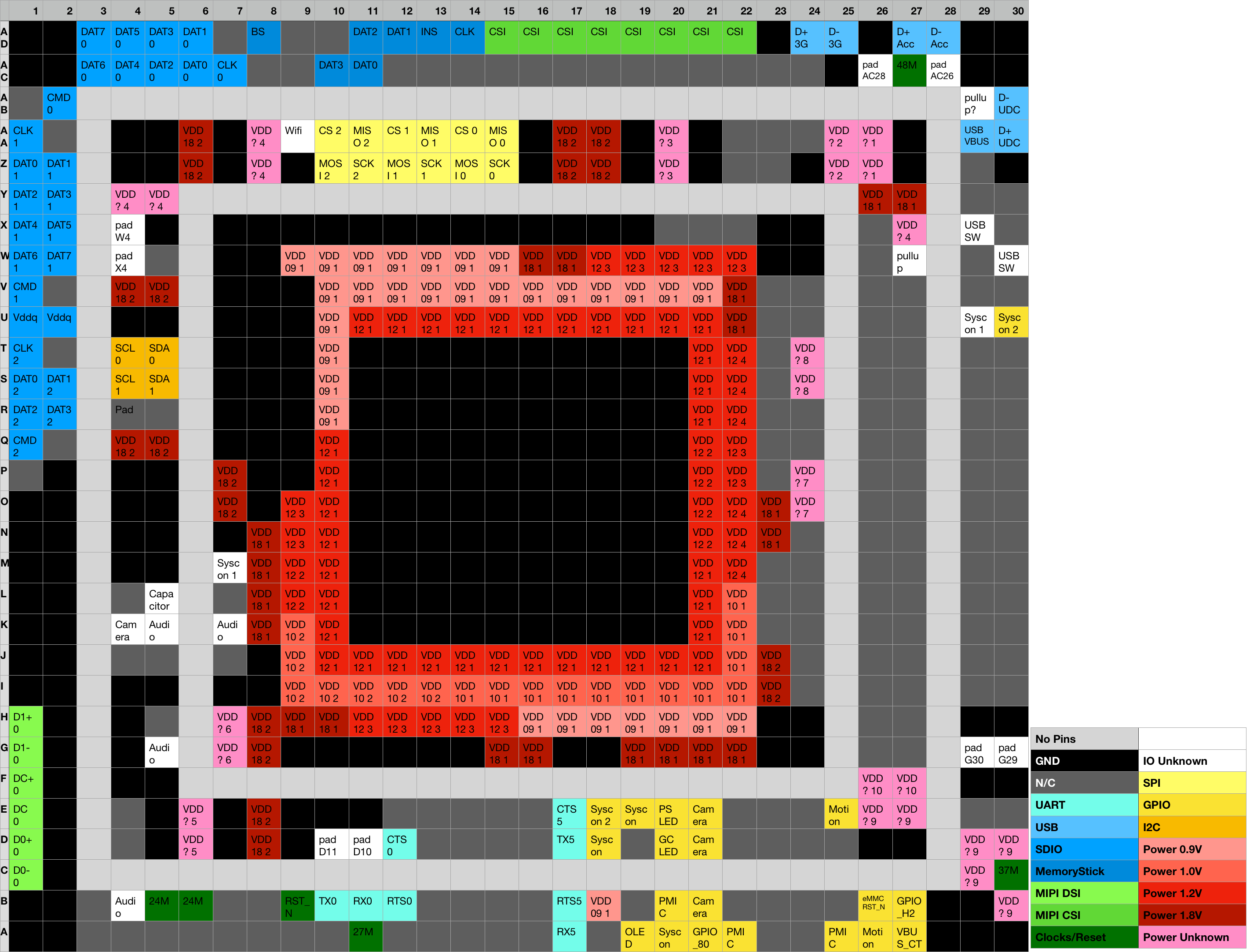
Pinout

The pinout is mostly reversed from the PCB delayer and is based off of PCH-1XXX on the IRS-002 board. It may not include some pins only used in other PS Vita models.
UART
See UART Console for pinout and UART Registers for programming.
| Name |
Pin |
Description
|
| CTS0 |
D12 |
UART0 clear to send
|
| RTS0 |
B12 |
UART0 request to send
|
| TX0 |
B10 |
UART0 transmit
|
| RX0 |
B11 |
UART0 receive
|
| CTS5 |
E17 |
UART5 clear to send
|
| RTS5 |
B17 |
UART5 request to send
|
| TX5 |
D17 |
UART5 transmit
|
| RX5 |
A17 |
UART5 receive
|
USB
See EHCI.
| Name |
Pin |
Description
|
| D+ 3G |
AD24 |
3G modem USB D+ (host EHCI)
|
| D- 3G |
AD25 |
3G modem USB D (host EHCI)
|
| D+ Acc |
AD27 |
Accessory port USB D+ (host EHCI)
|
| D- Acc |
AD28 |
Accessory port USB D (host EHCI)
|
| D+ UDC |
AA30 |
Multiconnector USB D+ (client, OTG maybe supported)
|
| D- UDC |
AB30 |
Multiconnector USB D (client, OTG maybe supported)
|
| USB VBUS |
AA29 |
Also goes to SN99057
|
SDIO
See SceSdif.
| Name |
Pin |
Description
|
| CLK 0 |
AC7 |
eMMC clock
|
| CMD 0 |
AB2 |
eMMC CMD
|
| DAT0 0 |
AC6 |
eMMC DAT0
|
| DAT1 0 |
AD6 |
eMMC DAT1
|
| DAT2 0 |
AC5 |
eMMC DAT2
|
| DAT3 0 |
AD5 |
eMMC DAT3
|
| DAT4 0 |
AC4 |
eMMC DAT4
|
| DAT5 0 |
AD4 |
eMMC DAT5
|
| DAT6 0 |
AC3 |
eMMC DAT6
|
| DAT7 0 |
AD3 |
eMMC DAT7
|
| CLK 1 |
AA1 |
Gamecard clock
|
| CMD 1 |
V1 |
Gamecard CMD
|
| DAT0 1 |
Z1 |
Gamecard DAT0
|
| DAT1 1 |
Z2 |
Gamecard DAT1
|
| DAT2 1 |
Y1 |
Gamecard DAT2
|
| DAT3 1 |
Y2 |
Gamecard DAT3
|
| DAT4 1 |
X1 |
Gamecard DAT4 (unused)
|
| DAT5 1 |
X2 |
Gamecard DAT5 (unused)
|
| DAT6 1 |
W1 |
Gamecard DAT6 (unused)
|
| DAT7 1 |
W2 |
Gamecard DAT7 (unused)
|
| CLK 2 |
T1 |
Wlan/Bt clock
|
| CMD 2 |
Q1 |
Wlan/Bt CMD
|
| DAT0 2 |
S1 |
Wlan/Bt DAT0
|
| DAT1 2 |
S2 |
Wlan/Bt DAT1
|
| DAT2 2 |
R1 |
Wlan/Bt DAT2
|
| DAT3 2 |
R2 |
Wlan/Bt DAT3
|
| Vddq |
U1 |
SDIO voltage regulation
|
| Vddq |
U2 |
SDIO voltage regulation
|
MS
See MSIF Registers.
| Name |
Pin |
Description
|
| CLK |
AD14 |
Memorycard CLK
|
| INS |
AD13 |
Memorycard insert detect
|
| BS |
AD8 |
Memorycard bus state (select bit)
|
| DAT0 |
AC11 |
Memorycard DAT0
|
| DAT1 |
AD12 |
Memorycard DAT1
|
| DAT2 |
AD11 |
Memorycard DAT2
|
| DAT3 |
AC10 |
Memorycard DAT3
|
MIPI DSI
See DSI Registers.
| Name |
Pin |
Description
|
| DC+ 0 |
F1 |
Internal display clock lane
|
| DC- 0 |
E1 |
Internal display clock lane
|
| D0+ 0 |
D1 |
Internal display data 0 lane
|
| D0- 0 |
C1 |
Internal display data 0 lane
|
| D1+ 0 |
H1 |
Internal display data 1 lane
|
| D1- 0 |
G1 |
Internal display data 1 lane
|
MIPI CSI
| Name |
Pin |
Description
|
|
AD15 |
Front/back camera
|
|
AD16 |
Front/back camera
|
|
AD17 |
Front/back camera
|
|
AD18 |
Front/back camera
|
|
AD19 |
Front/back camera
|
|
AD20 |
Front/back camera
|
|
AD21 |
Front/back camera
|
|
AD22 |
Front/back camera
|
SPI
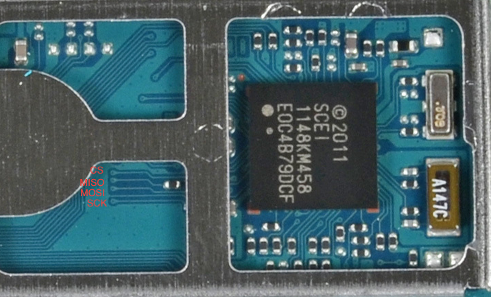
 SPI0 (Syscon) trace. Termination resistor under the shield. See SPI Registers.
| Name |
Pin |
Description
|
| CS 0 |
AA14 |
Syscon SPI chip select
|
| SCK 0 |
Z15 |
Syscon SPI clock
|
| MISO 0 |
AA15 |
Syscon SPI output
|
| MOSI 0 |
Z14 |
Syscon SPI input
|
| CS 1 |
AA12 |
Motion (accelerometer IC) SPI chip select
|
| SCK 1 |
Z13 |
Motion (accelerometer IC) SPI clock
|
| MISO 1 |
AA13 |
Motion (accelerometer IC) SPI output
|
| MOSI 1 |
Z12 |
Motion (accelerometer IC) SPI input
|
| CS 2 |
AA10 |
P1P40167 clock synthesizer SPI chip select
|
| SCK 2 |
Z11 |
P1P40167 clock synthesizer SPI clock
|
| MISO 2 |
AA11 |
P1P40167 clock synthesizer SPI output
|
| MOSI 2 |
Z10 |
P1P40167 clock synthesizer SPI input
|
GPIO
See GPIO Registers.
| Name |
Pin |
Description
|
| Syscon |
D18 |
To syscon
|
| Syscon |
E18 |
To syscon
|
| Syscon |
E19 |
To syscon
|
| Syscon |
A20 |
To syscon
|
| Motion |
E25 |
To Motion (accelerometer IC)
|
| Motion |
A26 |
To Motion (accelerometer IC)
|
| Camera |
E21 |
To camera
|
| Camera |
D21 |
To camera
|
| Camera |
B21 |
To camera
|
| PS LED |
E20 |
To transistor gate powering PS button LED
|
| GC LED |
D20 |
To LED next to gamecard port
|
| PMIC |
A22 |
To PMIC
|
| PMIC |
A25 |
To PMIC
|
| PMIC |
B20 |
To PMIC
|
| OLED |
A19 |
To OLED connector port
|
| GPIO_80 |
A21 |
3G modem pin 23
|
| GPIO_H2 |
B27 |
3G modem pin 11
|
| VBUS_CTRL |
A27 |
3G modem pin 17
|
| eMMC RST_N |
B26 |
RST_N of eMMC
|
I2C
See I2C Registers.
| Name |
Pin |
Description
|
| SCL 0 |
T4 |
I2C0 clock
|
| SDA 0 |
T5 |
I2C0 data
|
| SCL 1 |
S4 |
I2C1 clock
|
| SDA 1 |
S5 |
I2C1 data
|
Misc
| Name |
Pin |
Description
|
| pad AC28 |
AC26 |
Goes to pad with passive, grouped with AC28?
|
| pad AC26 |
AC28 |
Goes to pad with passive, grouped with AC26?
|
| pullup? |
AB29 |
Goes to a pullup resistor?
|
| Wlan/Bt |
AA9 |
Goes to Wlan/Bt SoC
|
| pad W4 |
X4 |
Goes to pad, connects with W4
|
| pad X4 |
W4 |
Goes to pad, connects with X4
|
| pullup X27 |
W27 |
Pullup resistor to X27
|
|
X29 |
Goes near PMIC
|
|
X30 |
Goes near PMIC
|
| pad M7 |
U29 |
Connects to M7 with a passive
|
| rst? |
U30 |
Goes near PMIC, might be reset
|
| pad U29 |
M7 |
Connects to U29 with a passive
|
| Capacitor |
L5 |
Goes to a capacitor, voltage regulation?
|
| Camera |
K4 |
Goes to camera, camera audio input?
|
| Audio |
K5 |
Maybe I2S
|
| Audio |
K7 |
Maybe I2S
|
| Audio |
G5 |
Maybe I2S
|
| Audio |
B4 |
Maybe I2S
|
| Syscon |
B9 |
Goes to syscon
|
| pad D11 |
D10 |
Connects to D10 through passive
|
| pad D10 |
D11 |
Connects to D11 through passive
|
| pad G30 |
G29 |
Connects to G30 through passive
|
| pad G29 |
G30 |
Connects to G29 through passive
|
Clocks/Reset
See Pervasive.
| Name |
Pin |
Description
|
| 24M |
B5 |
24.576MHz, suspected audio related
|
| 24M |
B6 |
24.576MHz, suspected audio related
|
| 27M |
A11 |
27MHz, suspected input to main PLL
|
| 48M |
AC27 |
48MHz, SD controller
|
| 37M |
C30 |
37MHz, suspected main clock
|
| RST_N |
B9 |
Held for 20ms on startup by Syscon, 100K pulldown
|
Power
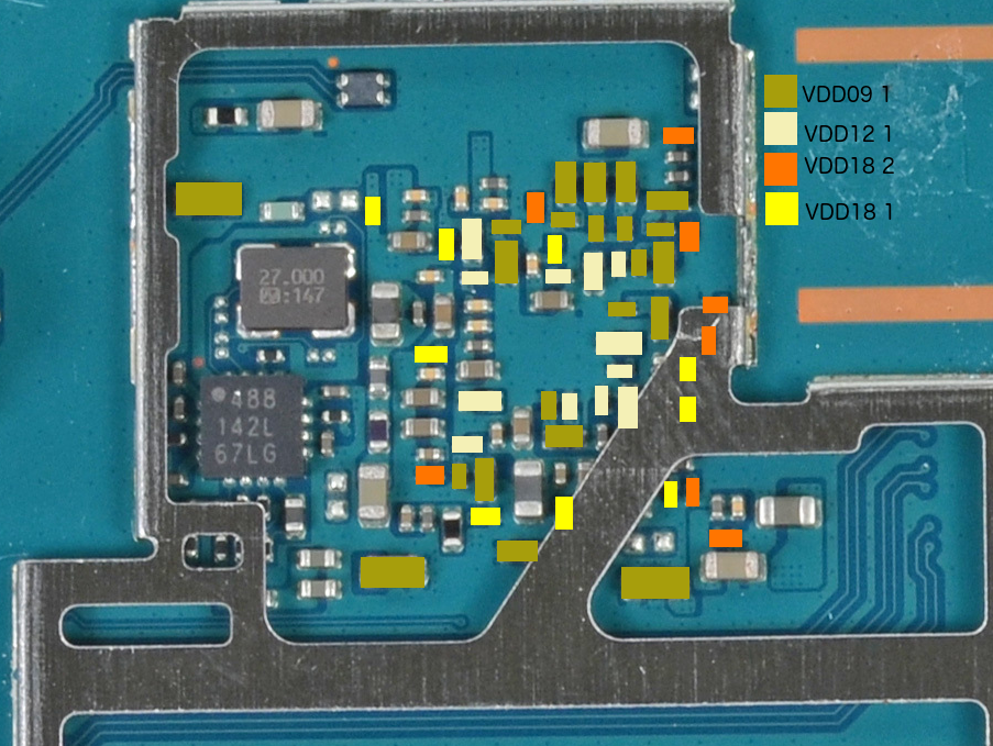
Different power domains are numbered. Some voltages are unknown.
 Decoupling capacitors for some major power domains are shown.
| Name |
Pin |
Description
|
| VDD09 1 |
W9 |
0.9V power domain 1
|
| VDD09 1 |
W10 |
0.9V power domain 1
|
| VDD09 1 |
W11 |
0.9V power domain 1
|
| VDD09 1 |
W12 |
0.9V power domain 1
|
| VDD09 1 |
W13 |
0.9V power domain 1
|
| VDD09 1 |
W14 |
0.9V power domain 1
|
| VDD09 1 |
W15 |
0.9V power domain 1
|
| VDD09 1 |
V10 |
0.9V power domain 1
|
| VDD09 1 |
V11 |
0.9V power domain 1
|
| VDD09 1 |
V12 |
0.9V power domain 1
|
| VDD09 1 |
V13 |
0.9V power domain 1
|
| VDD09 1 |
V14 |
0.9V power domain 1
|
| VDD09 1 |
V15 |
0.9V power domain 1
|
| VDD09 1 |
V16 |
0.9V power domain 1
|
| VDD09 1 |
V17 |
0.9V power domain 1
|
| VDD09 1 |
V18 |
0.9V power domain 1
|
| VDD09 1 |
V19 |
0.9V power domain 1
|
| VDD09 1 |
V20 |
0.9V power domain 1
|
| VDD09 1 |
V21 |
0.9V power domain 1
|
| VDD09 1 |
U10 |
0.9V power domain 1
|
| VDD09 1 |
T10 |
0.9V power domain 1
|
| VDD09 1 |
S10 |
0.9V power domain 1
|
| VDD09 1 |
R10 |
0.9V power domain 1
|
| VDD09 1 |
H16 |
0.9V power domain 1
|
| VDD09 1 |
H17 |
0.9V power domain 1
|
| VDD09 1 |
H18 |
0.9V power domain 1
|
| VDD09 1 |
H19 |
0.9V power domain 1
|
| VDD09 1 |
H20 |
0.9V power domain 1
|
| VDD09 1 |
H21 |
0.9V power domain 1
|
| VDD09 1 |
H22 |
0.9V power domain 1
|
| VDD09 1 |
B18 |
0.9V power domain 1
|
| VDD10 1 |
K9 |
1.0V power domain 1
|
| VDD10 1 |
J9 |
1.0V power domain 1
|
| VDD10 1 |
I9 |
1.0V power domain 1
|
| VDD10 1 |
I10 |
1.0V power domain 1
|
| VDD10 1 |
I11 |
1.0V power domain 1
|
| VDD10 1 |
I12 |
1.0V power domain 1
|
| VDD10 1 |
I13 |
1.0V power domain 1
|
| VDD10 2 |
I14 |
1.0V power domain 2
|
| VDD10 2 |
I15 |
1.0V power domain 2
|
| VDD10 2 |
I16 |
1.0V power domain 2
|
| VDD10 2 |
I17 |
1.0V power domain 2
|
| VDD10 2 |
I18 |
1.0V power domain 2
|
| VDD10 2 |
I19 |
1.0V power domain 2
|
| VDD10 2 |
I20 |
1.0V power domain 2
|
| VDD10 2 |
I21 |
1.0V power domain 2
|
| VDD10 2 |
I22 |
1.0V power domain 2
|
| VDD10 2 |
J22 |
1.0V power domain 2
|
| VDD10 2 |
K22 |
1.0V power domain 2
|
| VDD10 2 |
L22 |
1.0V power domain 2
|
| VDD12 1 |
U11 |
1.2V power domain 1 (main core power)
|
| VDD12 1 |
U12 |
1.2V power domain 1 (main core power)
|
| VDD12 1 |
U13 |
1.2V power domain 1 (main core power)
|
| VDD12 1 |
U14 |
1.2V power domain 1 (main core power)
|
| VDD12 1 |
U15 |
1.2V power domain 1 (main core power)
|
| VDD12 1 |
U16 |
1.2V power domain 1 (main core power)
|
| VDD12 1 |
U17 |
1.2V power domain 1 (main core power)
|
| VDD12 1 |
U18 |
1.2V power domain 1 (main core power)
|
| VDD12 1 |
U19 |
1.2V power domain 1 (main core power)
|
| VDD12 1 |
U20 |
1.2V power domain 1 (main core power)
|
| VDD12 1 |
U21 |
1.2V power domain 1 (main core power)
|
| VDD12 1 |
U22 |
1.2V power domain 1 (main core power)
|
| VDD12 1 |
T22 |
1.2V power domain 1 (main core power)
|
| VDD12 1 |
S22 |
1.2V power domain 1 (main core power)
|
| VDD12 1 |
R22 |
1.2V power domain 1 (main core power)
|
| VDD12 1 |
M22 |
1.2V power domain 1 (main core power)
|
| VDD12 1 |
L22 |
1.2V power domain 1 (main core power)
|
| VDD12 1 |
K22 |
1.2V power domain 1 (main core power)
|
| VDD12 1 |
J22 |
1.2V power domain 1 (main core power)
|
| VDD12 1 |
J21 |
1.2V power domain 1 (main core power)
|
| VDD12 1 |
J20 |
1.2V power domain 1 (main core power)
|
| VDD12 1 |
J19 |
1.2V power domain 1 (main core power)
|
| VDD12 1 |
J18 |
1.2V power domain 1 (main core power)
|
| VDD12 1 |
J17 |
1.2V power domain 1 (main core power)
|
| VDD12 1 |
J16 |
1.2V power domain 1 (main core power)
|
| VDD12 1 |
J15 |
1.2V power domain 1 (main core power)
|
| VDD12 1 |
J14 |
1.2V power domain 1 (main core power)
|
| VDD12 1 |
J13 |
1.2V power domain 1 (main core power)
|
| VDD12 1 |
J12 |
1.2V power domain 1 (main core power)
|
| VDD12 1 |
J11 |
1.2V power domain 1 (main core power)
|
| VDD12 1 |
J10 |
1.2V power domain 1 (main core power)
|
| VDD12 1 |
K10 |
1.2V power domain 1 (main core power)
|
| VDD12 1 |
L10 |
1.2V power domain 1 (main core power)
|
| VDD12 1 |
M10 |
1.2V power domain 1 (main core power)
|
| VDD12 1 |
N10 |
1.2V power domain 1 (main core power)
|
| VDD12 1 |
O10 |
1.2V power domain 1 (main core power)
|
| VDD12 1 |
P10 |
1.2V power domain 1 (main core power)
|
| VDD12 1 |
Q10 |
1.2V power domain 1 (main core power)
|
| VDD12 2 |
M9 |
1.2V power domain 2
|
| VDD12 2 |
L9 |
1.2V power domain 2
|
| VDD12 2 |
Q21 |
1.2V power domain 2
|
| VDD12 2 |
P21 |
1.2V power domain 2
|
| VDD12 2 |
O21 |
1.2V power domain 2
|
| VDD12 2 |
N21 |
1.2V power domain 2
|
| VDD12 3 |
W18 |
1.2V power domain 3
|
| VDD12 3 |
W19 |
1.2V power domain 3
|
| VDD12 3 |
W20 |
1.2V power domain 3
|
| VDD12 3 |
W21 |
1.2V power domain 3
|
| VDD12 3 |
W22 |
1.2V power domain 3
|
| VDD12 3 |
Q22 |
1.2V power domain 3
|
| VDD12 3 |
P22 |
1.2V power domain 3
|
| VDD12 3 |
O9 |
1.2V power domain 3
|
| VDD12 3 |
N9 |
1.2V power domain 3
|
| VDD12 3 |
H11 |
1.2V power domain 3
|
| VDD12 3 |
H12 |
1.2V power domain 3
|
| VDD12 3 |
H13 |
1.2V power domain 3
|
| VDD12 3 |
H14 |
1.2V power domain 3
|
| VDD12 3 |
H15 |
1.2V power domain 3
|
| VDD12 4 |
T22 |
1.2V power domain 4
|
| VDD12 4 |
S22 |
1.2V power domain 4
|
| VDD12 4 |
R22 |
1.2V power domain 4
|
| VDD12 4 |
O22 |
1.2V power domain 4
|
| VDD12 4 |
N22 |
1.2V power domain 4
|
| VDD12 4 |
M22 |
1.2V power domain 4
|
| VDD18 1 |
Y26 |
1.8V power domain 1
|
| VDD18 1 |
Y27 |
1.8V power domain 1
|
| VDD18 1 |
N8 |
1.8V power domain 1
|
| VDD18 1 |
M8 |
1.8V power domain 1
|
| VDD18 1 |
L8 |
1.8V power domain 1
|
| VDD18 1 |
K8 |
1.8V power domain 1
|
| VDD18 1 |
O23 |
1.8V power domain 1
|
| VDD18 1 |
N23 |
1.8V power domain 1
|
| VDD18 1 |
H9 |
1.8V power domain 1
|
| VDD18 1 |
H10 |
1.8V power domain 1
|
| VDD18 1 |
G15 |
1.8V power domain 1
|
| VDD18 1 |
G16 |
1.8V power domain 1
|
| VDD18 1 |
G19 |
1.8V power domain 1
|
| VDD18 1 |
G20 |
1.8V power domain 1
|
| VDD18 1 |
G21 |
1.8V power domain 1
|
| VDD18 1 |
G22 |
1.8V power domain 1
|
| VDD18 1 |
W16 |
1.8V power domain 1
|
| VDD18 1 |
W17 |
1.8V power domain 1
|
| VDD18 1 |
V22 |
1.8V power domain 1
|
| VDD18 1 |
U22 |
1.8V power domain 1
|
| VDD18 2 |
AA6 |
1.8V power domain 2
|
| VDD18 2 |
Z6 |
1.8V power domain 2
|
| VDD18 2 |
AA17 |
1.8V power domain 2
|
| VDD18 2 |
Z17 |
1.8V power domain 2
|
| VDD18 2 |
AA18 |
1.8V power domain 2
|
| VDD18 2 |
Z18 |
1.8V power domain 2
|
| VDD18 2 |
V4 |
1.8V power domain 2
|
| VDD18 2 |
V5 |
1.8V power domain 2
|
| VDD18 2 |
P7 |
1.8V power domain 2
|
| VDD18 2 |
O7 |
1.8V power domain 2
|
| VDD18 2 |
J23 |
1.8V power domain 2
|
| VDD18 2 |
I23 |
1.8V power domain 2
|
| VDD18 2 |
H8 |
1.8V power domain 2
|
| VDD18 2 |
G8 |
1.8V power domain 2
|
| VDD18 2 |
E8 |
1.8V power domain 2
|
| VDD18 2 |
D8 |
1.8V power domain 2
|
| VDD? 1 |
AA26 |
Unknown power
|
| VDD? 1 |
Z26 |
Unknown power
|
| VDD? 2 |
AA25 |
Unknown power
|
| VDD? 2 |
Z25 |
Unknown power
|
| VDD? 3 |
AA20 |
Unknown power
|
| VDD? 3 |
Z20 |
Unknown power
|
| VDD? 4 |
AA8 |
Unknown power
|
| VDD? 4 |
Z8 |
Unknown power
|
| VDD? 4 |
Y4 |
Unknown power
|
| VDD? 4 |
Y5 |
Unknown power
|
| VDD? 4 |
X27 |
Unknown power
|
| VDD? 5 |
E6 |
Unknown power
|
| VDD? 5 |
D6 |
Unknown power
|
| VDD? 6 |
H7 |
Unknown power
|
| VDD? 6 |
G7 |
Unknown power
|
| VDD? 7 |
P24 |
Unknown power
|
| VDD? 7 |
O24 |
Unknown power
|
| VDD? 8 |
T24 |
Unknown power
|
| VDD? 8 |
S24 |
Unknown power
|
| VDD? 9 |
E26 |
Unknown power
|
| VDD? 9 |
E27 |
Unknown power
|
| VDD? 9 |
D29 |
Unknown power
|
| VDD? 9 |
D30 |
Unknown power
|
| VDD? 9 |
C29 |
Unknown power
|
| VDD? 9 |
B30 |
Unknown power
|
| VDD? 10 |
F26 |
Unknown power
|
| VDD? 10 |
F27 |
Unknown power
|
|
